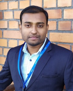
 Assistant Professor
Department of Electronics and Communication Engineering
National Institute of Technology Silchar
ACADEMIC QUALIFICATIONS
- B.E. : RTM Nagpur University, Nagpur, India, 2014
- Ph.D. : Indian Institute of Technology Patna, India, 2020
EXPERIENCE
- July 2022 – Till date: Assistant Professor Grade-II, National Institute of Technology (NIT) Silchar, Assam, 788010, India
- July 2021 – July 2022: Assistant Professor, Thapar Institute of Engineering & Technology (Deemed to be University), Patiala, Punjab, 147004, India
RESEARCH OPPORTUNITIES
- Ph.D. positions available under Institute Fellowship (Vacancy = 02)
- PhD position under Inspire Fellowship Awardees/ UGC-CSIR-NET(JRF) /Part-time category are also available.
RESEARCH INTERESTs AND SPECIALIZATION
- SPICE/Compact modeling of Bulk/SOI MOSFET, Multigate FET, Nanowire, Nanosheet/Nanaotube devices
- TCAD Simulation of nanoscale and emerging transistor architectures
- Analog circuits design and analysis
- Computational Nanoelectronics/Quantum modeling
- Statistical analysis of Reliability issues/Self-heating/Stress
- Machine learning based device modeling
- Non-volatile memory/RRAM/SRAM/Memristor
SHORT BIOGRAPHICAL SKETCH
Dr. Arun Kumar is presently working as an Assistant Professor in the ECE Department, National Institute of Technology, Silchar since July 2022. Dr. Arun has received his Ph.D. degree in Microelectronics from IIT Patna, India in 2020. Prior to joining NIT Silchar, he had worked as an Assistant Professor in the ECE Department, TIET, Patiala, India. He was awarded junior research fellowship and Senior research fellowship by CSIR, Government of India in 2016 and 2018, respectively. Dr. Arun is receipient of Foreign travel grant from CSIR, International travel grant from SERB, Govt. of India. Dr. Arun has published several research papers in reputed Journals and presented his research work at flagship IEEE conferences in India and abroad.
PROJECT(S)
- Compact model development for sub 7-nm NSFETs, SERB, Govt. of India, under NPDF, INR 19.20 Lakhs (Could not avail)
- Compact modeling and quantum transport simulation NSFETs for next generation circuit applications, TIET , Patiala, (2022), INR 4 Lakhs
BOOKS/CHAPTERS
- Arun Kumar, and Pramod Kumar Tiwari, Silicon Nanotube FETs: From device concept to analytical model development, Cutting-Edge Research on Low-Dimensional Nanoelectronic Devices: Physics and Material Science Aspects, Apple Academic Press, USA, (ISBN: 9781774638668).
PUBLICATION (JOURNALS)
- Arun Kumar, Shiv Bhushan, and Pramod Kumar Tiwari, “A Threshold Voltage Model of Silicon- Nanotube Based Ultra-Thin Double Gate-All-Around (DGAA) MOSFETs Incorporating Quantum Confinement Effects,” IEEE Transactions on Nanotechnology, vol. 16, no. 5 , pp 868-875, Sept. 2017.
- Arun Kumar, Shiv Bhushan, and Pramod Kumar Tiwari, “Analytical modeling of subthreshold characteristics of ultra-thin double gate-all-around (DGAA) MOSFETs incorporating quantum confinement effects,” Superlattices and Microstructures, vol. 109, pp. 567-578, May 2017.
- Arun Kumar, Pramod Kumar Tiwari “An Explicit Unified Drain Current Model for Silicon-Nanotube- Based Ultrathin Double Gate-All-Around MOSFETs” IEEE Transactions on Nanotechnology, vol. 17, no. 6,, pp 1224-1234, Nov. 2018.
- Arun Kumar, Shiv Bhushan, and Pramod Kumar Tiwari “Drain current modeling of double gate-all- around (DGAA) MOSFETs”, IET Circuits, Devices & Systems, vol. 13, no. 4, pp. 519-525, July 2019.
- Arun Kumar, P.S.T.N. Srinivas, and Pramod Kumar Tiwari, “An Insight into Self-heating Effects and its Implications on Hot Carrier Degradation for Silicon-Nanotube-based double gate-all-around (DGAA) MOSFETs,” IEEE Journal of Electron Devices Society, vol. 7, pp. 1100-1108, Nov. 2019.
- Arun Kumar, P S T N Srinivas, S. Bhushan, S Dubey, Y K Singh and P. K. Tiwari “Threshold Voltage Modeling of Double Gate-All-Around Metal-Oxide-Semiconductor Field-Effect-Transistors (DGAA MOSFETs) Including the Fringing Field Effects”, Journal of Nanoelectronics and Optoelectronics, Vol. 14, pp. 1–10, Nov. 2019.
- P.S.T.N. Srinivas, Arun Kumar, and Pramod Kumar Tiwari, “A Threshold Voltage Model of Tri-Gate Schottky-Barrier (TGSB) Field-Effect-Transistors (FETs)” Silicon, Vol. 13, pp. 25–35 Jan. 2021.
- P.S.T.N. Srinivas, Arun Kumar, and Pramod Kumar Tiwari, “Self-heating Effects and Hot Carrier Degradation in In0.53Ga0.47As Gate-All-Around (GAA) MOSFETs” Semiconductor Science and Technology, Vol. 35, pp. 065008-1-8, May 2020.
- P.S.T.N. Srinivas, Arun Kumar, and Pramod Kumar Tiwari, “Effect of self-heating on small-signal parameters of In0.53Ga0.47As based gate-all-around MOSFETs” Semiconductor Science and Technology, Vol. 36, pp. 125012-1-8, Nov. 2021.
- Singh, S., Srinivas, P.S.T.N., Kumar, A. et al. Physical Insight into Self-heating Induced Performance Degradation in RingFET. Silicon (2021). https://doi.org/10.1007/s12633-021-01491-9
PUBLICATION (CONFERENCES)
- Arun Kumar, P.S.T.N. Srinivas, and Pramod Kumar Tiwari, ” Analytical Threshold Voltage Model of Schottky-source/drain (Schottky-S/D) double gate-all-around (DGAA) Field-Effect-Transistors (FETs),” 2019 IEEE Devices for Integrated Circuit (DevIC), Kalyani, March 2019.
- Arun Kumar, P.S.T.N. Srinivas, and Pramod Kumar Tiwari, “Physical Insight into Self-heating Effects in Ultra-thin Junctionless Gate-All-Around FETs,” 9th IEEE International Nanoelectronics Conference (INEC), Kuching, Malaysia, July 2019
- Arun Kumar, P.S.T.N. Srinivas, and Pramod Kumar Tiwari, “Compact Drain Current Model of Silicon- Nanotube-based Double Gate-All-Around (DGAA) MOSFETs Incorporating Short Channel Effects,” 14th IEEE Nanotechnology Materials and Devices Conference (NMDC), Stockholm, Oct. 2019
- Shiv Bhushan, Arun Kumar, Deepti Gola, and Pramod Kumar Tiwari, “An analytical subthreshold current model of short-channel symmetrical double gate-all- around (DGAA) field-effect-transistors” 2nd International conference 2017 Device for integrated circuits (DevIC), pp.8-12, 2017.
- P.S.T.N. Srinivas, Arun Kumar, and Pramod Kumar Tiwari, “Effects of Lateral Spreading in 2- Dimensional Non-Uniform Doped Junctionless FinFETs,” 9th IEEE International Nanoelectronics Conference (INEC), Kuching, Malayisia, July 2019
- Pramod Kumar Tiwari, Arun Kumar and Dipankar Talukdar, “An analytical gate tunneling current model of Re-S/D SOI MOSFETs,” 2016 IEEE Uttar Pradesh Section International Conference on Electrical, Computer and Electronics Engineering (UPCON), Varanasi, pp. 29-31, 2016.
- Arun Kumar, P.S.T.N. Srinivas, and Pramod Kumar Tiwari, “Analytical Modeling of Subthreshold Current and Subthreshold Swing of Schottky-Barrier Source/Drain Double Gate-All-Around (DGAA) MOSFETs” 5th IEEE iSES, Rourkela, 2019.
PROFESSIONAL MEMBERSHIPS
- Member, IEEE
- Member, IEEE Electron Device Society
- IEEE Young Professionals
- IEEE Nanotechnology Council
- Member, IEEE TechEthics Community
AWARDS & RECOGNITIONS
- 2015- CSIR-NET (JRF) with All India Rank-139
- 2014, 2015- Qualified Graduate Aptitude Test in Engineering
- 2016-2018, Junior Research Fellowship for PhD- CSIR, Government of India.
- 2018-2020, Senior Research Fellowship for PhD- CSIR, Government of India.
- 2019- International Travel Grant for 14th NMDC at Stockholm, Sweden- Science and Engineering Research Board (SERB), Government of India.
- 2019- International Travel Grant for 9th INEC at Kuching, Malaysia – Council of Scientific and Industrial Research (CSIR), Government of India.
- 2019- First position in Poster Presentation- Research Scholars’ Day, Indian Institute of Technology Patna.
- 2014 – University 2nd rank in B.E. Final Exam.
ADMINISTRATIVE RESPONSIBILITY
- Associate Warden, Visvesvaraya Hostel (Hostel No. 8), NIT Silchar (4th January 2023 – continue)
- Department Training & Placement Coordinator (11th August 2023 -continue)
Ph.D. Scholars
- K Mamota Devi (Ministry of Education (MoE) Fellowship, ongoing)
- Venkateswara Rao Busani (QIP Fellowship, ongoing)
- P Siva Durga Rao (Part-time, Ongoing)
M.Tech students
- Subhash Kumar
- Mohit Dutt Mathur
B.Tech. Projects
- G. Anith Chaudhary “Semiconductor device based Bio-sensor” – M.S (Analog and Mixed signal Design), Arizona State University, USA
- T. Sandeep Kumar, Anusha Hazarika ” Machine learning based Semiconductor device analysis”
